DOCUMENT NUMBER: REV:
M0420SD-204SDAR1-3
00
DATE PRINTED:
SHEET:
STANDARD NAME:
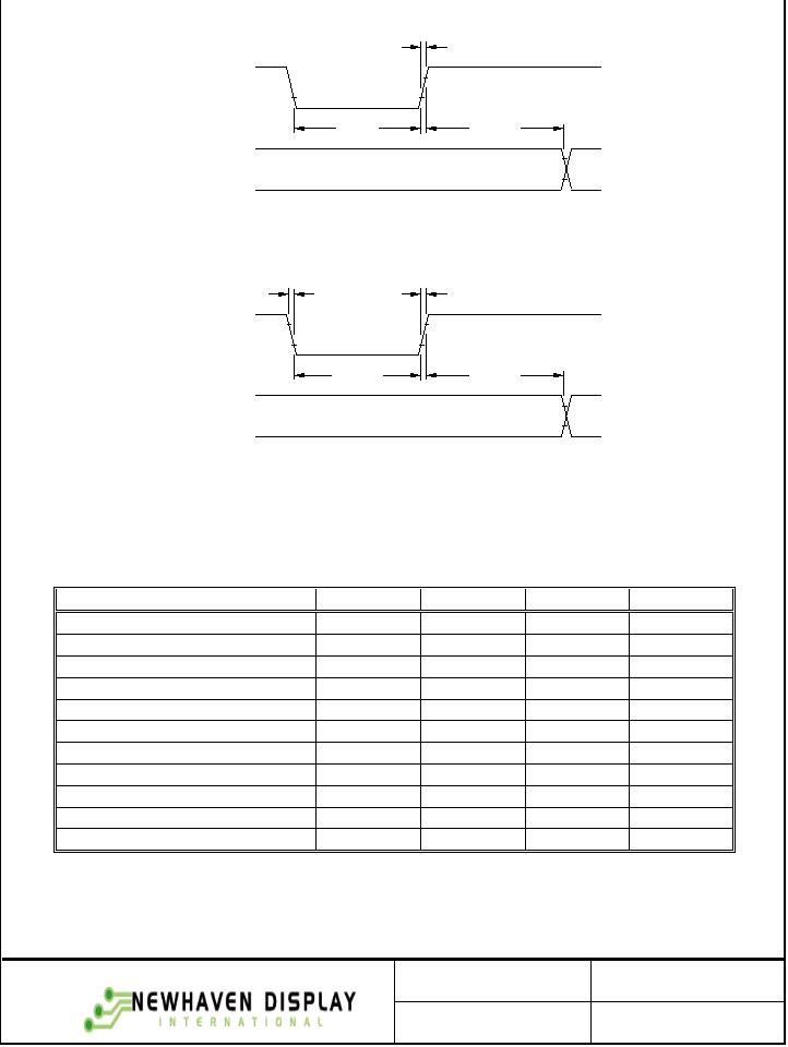
Vcc
0.2V
4.5V
t
OFF
RS, STB
t
IRSTD
t
RVCC
Figure 1.
Power-up Internal Reset Timing
RST/
t
RSTL
RS, STB
t
ERSTD
t
f
t
r
Figure 2.
External Reset Timing
4.7.2 MOTOROLA M68-TYPE PARALLEL INTERFACE TIMING
(See Figures 3 and 4)
Item
Symbol Min. Max. Unit
RS, R/W setup time
tAS
20
-
ns
RS, R/W hold time
tAH
10
-
ns
Input signal rise time
tr
-15ns
Input signal fall time
tf
-15ns
E pulse width high
PWEH
230
-
ns
E pulse width low
PWEL
230
-
ns
Write data setup time
tDS
80
-
ns
Write data hold time
tDH
10
-
ns
E cycle time
tCYCE
500
-
ns
Read data delay time
tDD
-
160 ns
Read data hold time
tDHR
5-ns
Note: All timing is specified using 20% and 80% of VCC
as the reference points.
7 of 24
发布紧急采购,3分钟左右您将得到回复。
相关PDF资料
M1MA142WAT1G
DIODE SW DUAL SS CA 80V SOT-323
M1MA142WKT1G
DIODE SW DUAL SS CC 80V SOT-323
M1MA152WAT1
DIODE SWITCH DUAL CA 80V SC59
M1MA152WKT1G
DIODE SWITCH DUAL CA 80V SC59
M2256PW
DISPLAY SCREEN 22" MULTI-TOUCH
M30L40C-E3/4W
DIODE SCHOTTKY 30A 40V TO-220AB
MAN6910
LED 7-SEG DUAL CA RED RHDP .56"
MB203LCD-1
LCD MOD W/CABLE/CONN FOR MB203A
相关代理商/技术参数
M0425SBA109
制造商:n/a 功能描述:Ships in 2 days
M04350012
制造商:Molex 功能描述:
M04-390DJ
制造商:Schurter Electronic Components 功能描述:DC SOCKET 1.05MM PCB JSBJ4 - Bulk
M0440HCZ933
制造商:n/a 功能描述:Ships in 2 days
M0445SC129
制造商:n/a 功能描述:Ships in 2 days
M045
制造商:Kemo Electronic 功能描述:Three Way Crossover
M0452/00
制造商:CHESIVALE ELECTRONICS 功能描述:TESTER TELEPHONE DSP COMPACT
M0459/01
制造商:CHESIVALE ELECTRONICS 功能描述:CORD SET BT
